
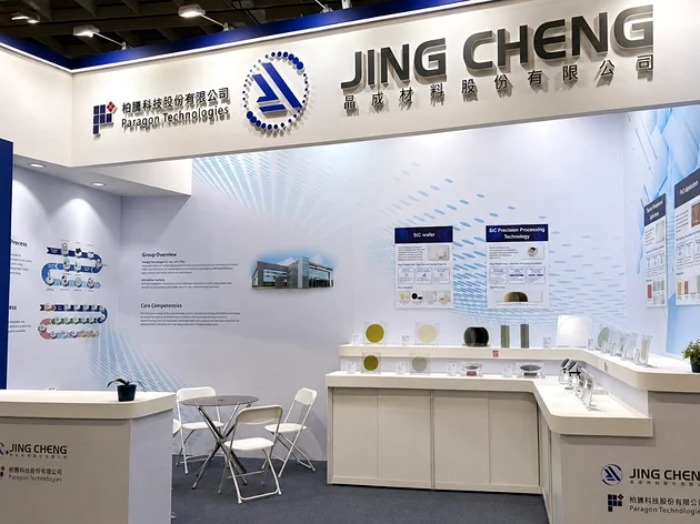
At SEMICON Taiwan 2026, Biotech showcased its advanced packaging applications.
Paragon and Jingcheng participated in SEMICON to showcase their titanium-copper seed layer coating technology for advanced packaging.

Bertech showcased advanced packaging applications at SEMICON Taiwan 2026. Photo provided by PARAGON
Economic Daily News Reporter Hsu Mu-Chun/Instant Report
PARAGON (3518) and its subsidiary Crystal Materials will jointly participate in SEMICON Taiwan 2026, the international semiconductor exhibition. Leveraging years of experience in vacuum vapor deposition (PVD) technology and material processing capabilities, Bertech continues to focus on high-power devices and advanced packaging applications. This time, they will showcase their key “titanium/copper seed layer” coating technology, with highlights covering silicon carbide (SiC) wafers, HDI substrates, ABF substrates, aluminum nitride (AlN) ceramic substrates, through-glass vias (TGV), silicon carbide through-hole vias (TSiCV), SiC microchannels, and other applications.
Titanium-Copper Seed Layer: A Key to Advanced Packaging Metallization
In the metallization process of advanced packaging and advanced substrates, the uniformity, continuity, and interfacial adhesion of the seed layer are crucial factors affecting the quality of subsequent copper plating and packaging reliability. Through optimized PVD process technology, Bertech can form titanium adhesive layers and copper conductive seed layers with excellent uniformity and adhesion on various substrates, thereby improving the interfacial quality between the metal layer and the substrate and meeting the stringent requirements of high-density interconnect structures for metallization processes.
Compared to some traditional wet metallization processes, PVD offers advantages such as dry processing and high film purity. Addressing the challenges of microvias and high aspect ratio structures, Bertech continues to optimize process parameters and plasma technology to improve the coverage, continuity, and adhesion of the seed layer. This advantage has been successfully extended to high-end materials such as ABF substrates and AlN ceramic substrates, further meeting the technological demands of ultra-fine line manufacturing.
Laying the Foundation for Next-Generation Packaging: From TGV to TSiCV
Beyond advanced substrate applications, PTTECH Technology is also actively showcasing its emerging and forward-looking applications to meet the demands of next-generation AI chip packaging for panel-level packaging and efficient heat dissipation. Glass substrates, due to their high flatness, dimensional stability, and excellent high-frequency electrical characteristics, are considered a highly promising next-generation substrate material for advanced packaging. PTTECH Technology has developed titanium-copper seed layer technology to address the adhesion between glass and metal and the metallization requirements of deep-hole structures. This technology continuously optimizes the film coverage and uniformity in microporous structures, laying the foundation for subsequent copper plating and redistribution layer (RDL) processes on glass substrates.
Simultaneously, for high-power SiC device applications, PTTECH Technology is also developing TSiCV and wafer back-side metallization (BGBM) processes. Through surface pretreatment and titanium-copper metallization technology, it improves the interface quality between the SiC substrate and the metal layer, thereby meeting the requirements of high-power devices for low-resistance metallization, high reliability, and packaging integration.

Substrate circuitry application. Photo provided by PTTECH Technology
Breaking through the high heat flux challenge: Wafer-level SiC microchannel cooling technology
Faced with the high heat flux challenges brought by high computing power and AI data centers, traditional air cooling and external liquid cooling solutions have limited heat dissipation capabilities for localized hot spots. Berton Technology combines the high thermal conductivity of SiC with precision processing technology to provide a “wafer-level microchannel” direct cooling solution. By integrating microchannels into the SiC substrate close to the heat source, the high thermal conductivity and excellent thermal stability of SiC materials can be leveraged to quickly eliminate temperature differences at hot spots, providing an ultimate solution for high-pressure microchannel heat dissipation.
Furthermore, the coefficient of thermal expansion of SiC is similar to that of silicon wafers, which helps reduce interfacial thermal stress, thereby reducing the risk of package structure warpage and interface delamination. With these characteristics, SiC microchannels are expected to meet the structural reliability requirements under coolant circulation and long-term operation, significantly improving the long-term reliability of advanced packaged devices.

SiC wafer regeneration and thinning applications. Photo provided by PTTECH Technology
PVD seed layer technology combined with SiC materials expands the supply chain footprint
PTTECH Technology, founded on its early EMI/ESD vacuum sputtering applications in 3C products, has actively invested in advanced process technology development in recent years. It possesses silicon carbide material supply, silicon carbide precision machining technology, and vacuum coating physical vapor deposition technology, providing comprehensive vertically integrated services from “front-end R&D and design” to “back-end mass production.” Simultaneously, through its subsidiary, Crystal Materials, it is developing and manufacturing SiC wafers, assembling a top-tier compound crystal expert team to create a high-specification, high-yield, vertically integrated one-stop production system.
The titanium-copper seed layer technology to be showcased at SEMICON Taiwan 2026 not only reflects PTTECH’s technological extension in dry coating processes but also demonstrates the company’s continued technological strength and strategic layout in penetrating the high-power device, advanced packaging, and third-generation semiconductor markets.